|
#1
 04-19-2008, 01:32 PM
|
|||
|
|||
|
I mentioned to Henry before I was originally considering dong a CPLD/SDRAM combo. I had looked at the PSRAM chip but passed it by due to not reading the datasheet close enough.... I thought it was a 16 bit only datapath, was 1.8v and of course the whole microbga thing was not that atttractive due to the whole mounting/rouitng issue.
I think PSRAM is still simpler from a login implmentation point of view in the CPLD and would still be the best choice if the cost of making PCB's and mounting the chip can be brought under control. ... but SDram is still an option. The chips is aprox $5 for the 128Mbit version. There are several IP cores out there that would most likely work out pretty well with some mods. The chip is TSOP II which has a .8mm spacing. To get enough i/o we are stiill probably looking at a cs132 package though for the cpld or a PQ208 which then makes the DIP option kind of hard to do. Last edited by rgjones; 04-19-2008 at 02:36 PM. 
|
|
#2
04-19-2008, 08:27 PM
|
|||
|
|||
|
I can't get the VFBGA54 to route with less than 4 layers. The benefit of the CPLD + SDRAM is that the board could be 2 layer AND the cost reduction in the SDRAM will help "pay" for the CPLD.
I had forgotten how hard the VFBGA was to route. MUCH harder than a 324BGA!!!
|
|
#3
04-19-2008, 09:16 PM
|
|||
|
|||
|
I have been playing around in eagle with the VFBGA 54 footprint and 4mil is pretty much a requirement afaict. Since only 4 pins are pwr/gnd ... it may still be possible to do a 2 layer board but all signals pretty much have to be hand routed beyond the chip.
|
|
#4
04-19-2008, 09:46 PM
|
|||
|
|||
|
I got it to route at 5 mil no problem. Does Eagle have a problem with 5?
|
|
#5
04-19-2008, 09:57 PM
|
|||
|
|||
|
From your examples Eagle doesn't do nearly as nice a job - ethier that or I don't have it setup right which is certanly a possibility.
ok .. I though for some reason there was only 12 mil beteen pads but it looks like there is 15 so 5 mil traces should go with 5 mil clearance on each side. Looks like i was (and still am doing somehting wrong ...but gettign a little farther) all signals routed easily with 5mil traces except the power signals. Its probably just a setting I missed. 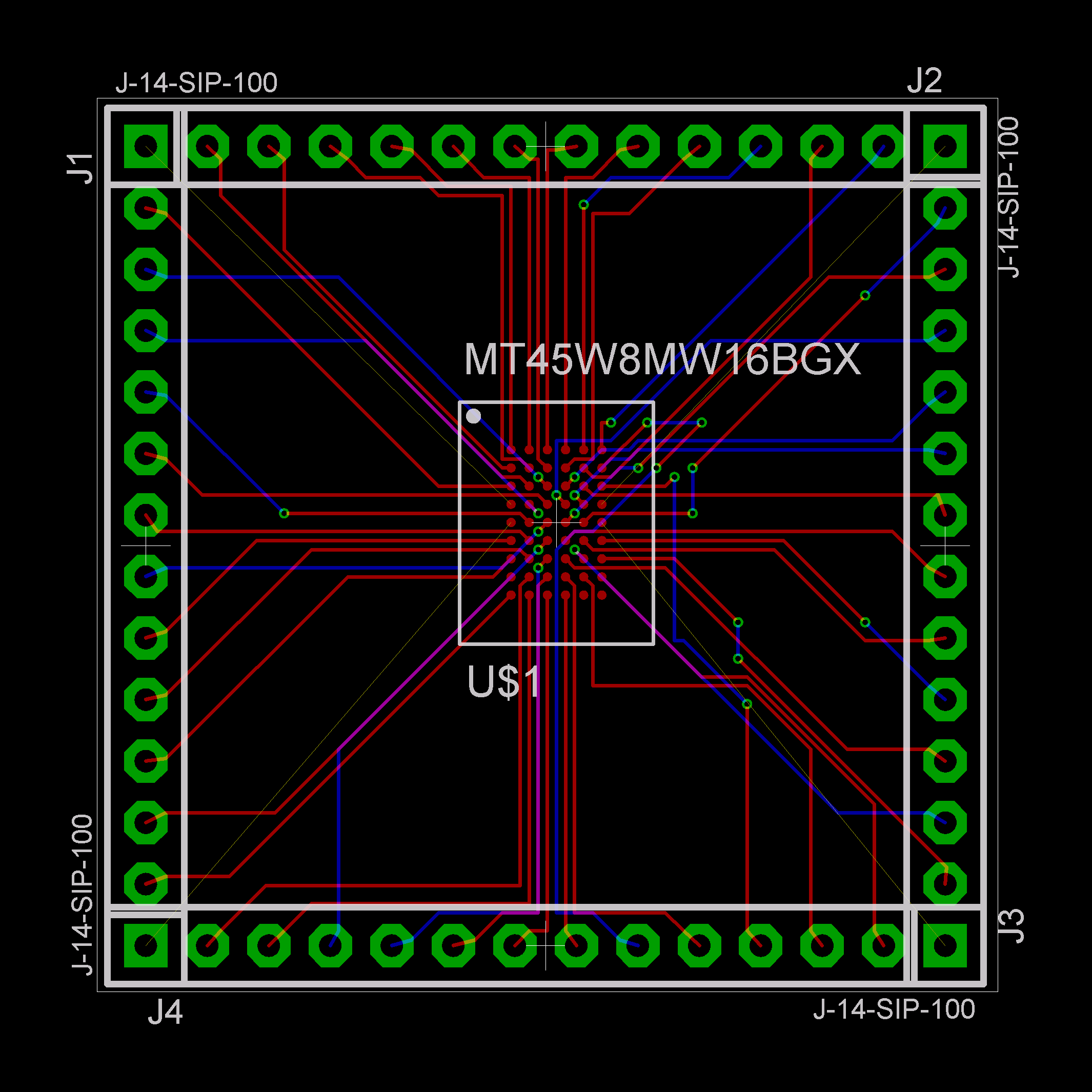
Last edited by rgjones; 04-19-2008 at 10:19 PM.
|
|
#6
04-19-2008, 10:14 PM
|
|||
|
|||
|
When I first made the board I had .37mm pads instead of .30mm. It didn't route any of the inner traces at 5 mil treace/space.
|
|
#7
04-19-2008, 10:32 PM
|
|||
|
|||
|
I also am using 8mil vias in the picture above but GP for example only allows min 12mil in there special prices quote (so going 8mil is going to cost extra)- not sure what the largest via is we can goto without hitting the 5mil clearance limit.
|
|
#9
04-21-2008, 09:45 PM
|
|||
|
|||
|
Since I didn't see these other threads till just now...
Grant: Can you email me those WinQ CAD files for the VFBGA Adapter and also produce and email the GERBER files too? I want to take a look at them and also get some pricing from QualityPCB.com. Glenn: FYI - I just received back some pricing for PCBs for a different project. Whole PCB Hard Gold plated: QualityPCB.com 10 PCBs - $218.28 25 PCBs - $253.52 Gold Phoenix Technology 10 PCBs - $179 25 PCBs - $280 So QualityPCB.com wins for larger orders. Wonder how they will do with that Adapter, not that price was 100% of the concern but I'd like to know for my notes. Soldering is still the major issue of course.
|
|
#10
04-21-2008, 11:24 PM
|
|||
|
|||
|
So it might be worth it to use GP for prototypes and QP for production runs. I have been meaning to learn how to panelize my own jobs so I can get different PCB's out of every run rather then just repeats of each design.
|
 |
|
|
 Similar Threads
|
||||
| Thread | Thread Starter | Forum | Replies | Last Post |
| Alternative D/C Board Fix!!!!! | Grant Stockly | Altair 680 | 0 | 06-03-2008 07:57 PM |


 Linear Mode

